Based on the information provided in the attached article, here are the key details about Cannabis ruderalis:
1. The concept of Cannabis ruderalis originated from a taxonomic error made by Schultes et al. They eschewed Vavilov’s earlier taxon C. sativa var. spontanea in favor of Janischevsky’s later synonym Cannabis ruderalis.
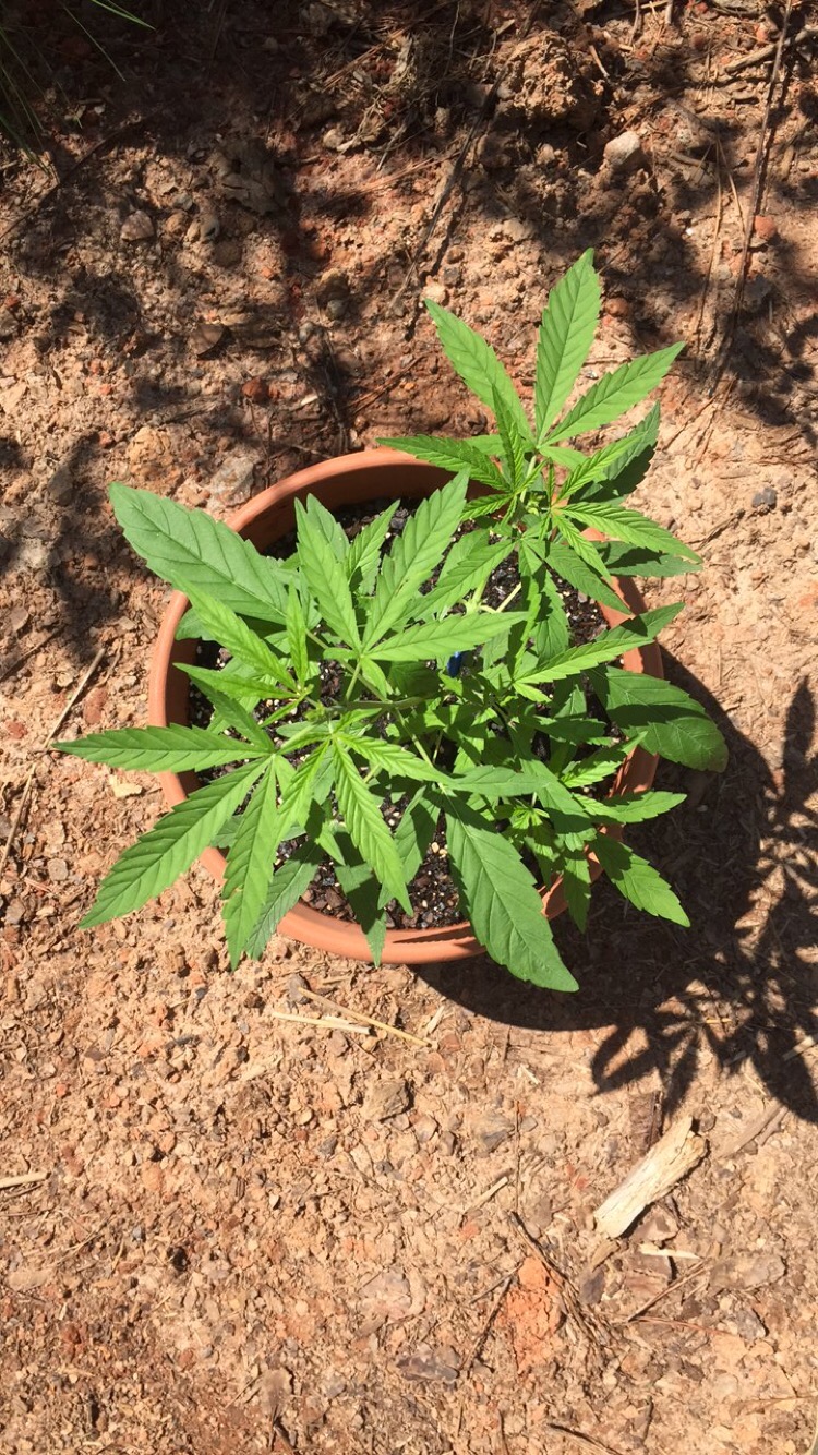
2. Schultes et al. departed from Janischevsky’s original concept of C. ruderalis. They applied the taxon to extremely short (≤0.61 m), unbranched plants with broad leaflets from Central Asia.
3. This contrasted with Janischevsky’s original description, which depicted relatively tall (up to 2.1 m), laxly branched plants with narrow leaflets from southeastern Europe.
4. Anderson illustrated a plant consistent with Schultes’ concept, not Janischevsky’s original description.
5. An early seed bank catalog showed “Ruderalis” plants growing near the Hungary-Ukraine border. These plants exhibited strong apical dominance and little branching, consistent with a spontaneous escape of cultivated hemp. This departed from both Vavilov’s and Janischevsky’s concepts.
6. In modern vernacular taxonomy, “Ruderalis” is applied to plants that exhibit one or more of these characteristics:
– CBD ≈ THC (roughly equal levels of CBD and THC)
– Wild-type morphology
– Early flowering (sometimes called “autoflowering” or day-neutral, meaning flowering is not induced by light cycle)
7. The article suggests that what is commonly referred to as “Ruderalis” is actually more closely aligned with C. sativa in formal botanical classification.
8. The author concludes that “Ruderalis,” along with “Sativa” and “Indica,” should be considered varieties of one species, Cannabis sativa L.
In summary, the concept of Cannabis ruderalis has evolved and been misapplied over time, leading to confusion between vernacular and formal taxonomies. The original description differs significantly from modern usage, and the term now encompasses a range of characteristics not initially associated with it.
Citations:
cannabis systematics at the levels of family genus and species